There is a rich and interesting history behind many of the iconic products we developed at Ten-Tec. Some of my former colleagues are silent keys now. For posterity, I want to share our story before it’s lost to the ether.
I worked for Ten-Tec for 22 years and helped develop many iconic products from receivers to kits, first joining in 1991 as an embedded Engineer. By 1996, I became head of Engineering and in 2001 I assumed the role of corporate Vice-President. A position I would hold until 2009, moving to remote work until 2013.. Throughout this time, I was also principal developer for all Ten-Tec Digital, DSP/SDR products and PC applications. For a list of products I helped design, click here.
Working at Ten-Tec was a labor of love. Ten-Tec President, Jack Burchfield (K4JU – SK) would often tell me that the reason he hired me was because of my letter telling him it was my dream job. I thoroughly enjoyed my time there and learned an infinite number of new skills and was able to help the company grow from through-hole technology, to surface mount and analog to digital.
I was also fortunate to work with a great team. Tom Salvetti, KC3NF Joined Ten-Tec as VP shortly after I started, taking over for Sid Kittrel who departed for health reasons. Lee Jones (WB4JTR – SK), a creatively brilliant RF engineer who was affectionately known by the nickname “kilowatt”. RF Engineer, Larry Boyd, ssss, who was also gifted with a knack for focusing on the details of product design. Engineering Technician, Boyd Lichlyter, had the incredible gift of troubleshooting designs, making things work while also having consummate skills with AUTOCAD and mechanical design.
Ten-Tec in Sevierville was a unique place to work for many reasons. Foremost was the completely flat-structure nature of the organization and its singular focus on producing the highest value products of the highest quality. Personnel turnover was near zero with most having done their jobs for a long time, decades in many cases.
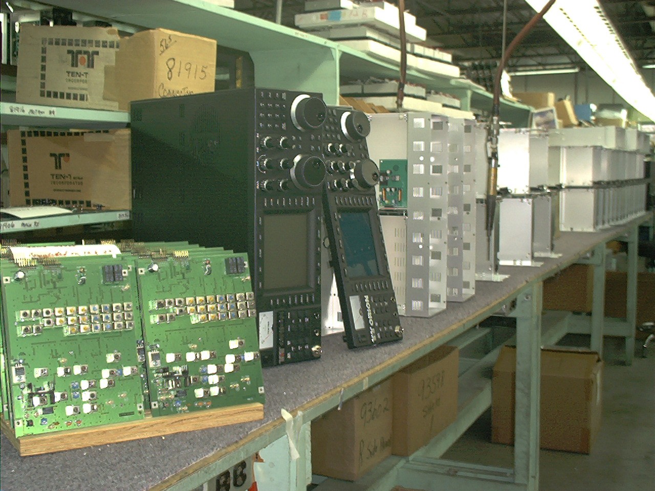
Ten-Tec was founded in 1968 and by the time I joined, it had by then become a vertically integrated company with nearly every activity taking place under one roof. Organizationally, outsourcing was never a first choice, with every effort made to keep work in the building. Over the years Ten-Tec had integrated not only electronic design but also raw PCB manufacturing, through-hole and SMD assembly, tool & die making, sheet metal punching, bending, painting, silk screening, along with manual printing and binding, all under one roof. All logically divided into 3 departments, namely Communications, Tool & Die and Metal Fab. Though internally focused, in addition to serving the core mission of producing Amateur Radios, each division served their own outside customers. With Tool & Die customers coming from the automotive and plastics industry and Metal Fabrication customers coming from various electronic industries. Later, we would add a division for electronic kits, under the T-Kits moniker. Inevitably, all resources are limited and subject to cost and value decisions. Such analysis would eventually lead to ending raw PCB manufacturing, discontinuance of T-kits and outsourcing of manual printing.
Because of the broad in-house capability, engineering and manufacturing processes had access to materials, processes and methods that may not be available had the processes been outsourced. This resulted in a Being able to instantly tap the different departments for creative solutions to solve problems or create products. Engineering personnel had generally unfettered access to these capabilities and most of us were trained on using the major equipment. This gave us first-hand knowledge of processes and materials that benefited us in product design.
A quick summary of in-house capability at Ten-Tec
PCB Manufacturing, including etching
Through-Hole Assembly Lines
SMD Assembly Lines with double sided capability
Tool & Die Design and Build
Programmable CNC Machines
Plastic Injection Machines
Enclosure Fabrication
RFI Shields and Covers
Powder Coat Painting
Solvent Based Painting
Screen Printing
Transformer Winding
Coil Winding
Perhaps the most amazing part of these capabilities is how it made quick turnarounds possible. Having near instant access to a wound coil, a metal part or a raw PCB contributed so much to the product design process. Often, these items could be made and delivered in hours. While, amazingly, it was not uncommon for the fab department to lament a process backup with “you’ll have it tomorrow.” In contrast, while working for another company, the lead time on such items was 12 to 16 weeks. A constant, immeasurable and frustrating drag on project momentum.

